
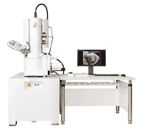
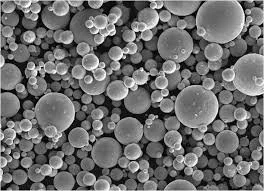
The JEOL JSM-IT800 SHL is a state-of-the-art Field Emission Scanning Electron Microscope (FE-SEM) designed for ultra-high-resolution imaging and microstructural characterization of a wide range of materials. Equipped with advanced field emission technology, the system delivers exceptional surface detail, nanoscale imaging, and analytical capabilities, making it ideal for materials science, biomaterials, nanotechnology, and life science research.
High-resolution field emission electron source
Ultra-high magnification imaging
Excellent low-voltage imaging performance
Large specimen chamber for versatile sample accommodation
Automated operation and intelligent navigation
High-depth-of-field imaging
Fast image acquisition and processing
User-friendly graphical interface
Compatible with EDS elemental analysis systems
Advanced imaging modes for detailed surface characterization
Surface morphology and microstructure analysis
Dental and biomaterials research
Nanomaterials characterization
Failure and fracture analysis
Thin film and coating evaluation
Particle size and shape analysis
Corrosion and wear studies
Semiconductor and electronic materials research
Biological specimen imaging
Additive manufacturing and advanced materials characterization
Nanoscale surface imaging
High-resolution topographical analysis
Elemental composition analysis (with EDS)
Microstructural characterization
Cross-sectional imaging
Particle and pore analysis
Quantitative image analysis
High-vacuum and low-vacuum observation modes
The JEOL JSM-IT800 SHL is a state-of-the-art Field Emission Scanning Electron Microscope (FE-SEM) designed for ultra-high-resolution imaging and microstructural characterization of a wide range of materials. Equipped with advanced field emission technology, the system delivers exceptional surface detail, nanoscale imaging, and analytical capabilities, making it ideal for materials science, biomaterials, nanotechnology, and life science research.
High-resolution field emission electron source
Ultra-high magnification imaging
Excellent low-voltage imaging performance
Large specimen chamber for versatile sample accommodation
Automated operation and intelligent navigation
High-depth-of-field imaging
Fast image acquisition and processing
User-friendly graphical interface
Compatible with EDS elemental analysis systems
Advanced imaging modes for detailed surface characterization
Surface morphology and microstructure analysis
Dental and biomaterials research
Nanomaterials characterization
Failure and fracture analysis
Thin film and coating evaluation
Particle size and shape analysis
Corrosion and wear studies
Semiconductor and electronic materials research
Biological specimen imaging
Additive manufacturing and advanced materials characterization
Nanoscale surface imaging
High-resolution topographical analysis
Elemental composition analysis (with EDS)
Microstructural characterization
Cross-sectional imaging
Particle and pore analysis
Quantitative image analysis
High-vacuum and low-vacuum observation modes